Features & Applications
HTCC Materials
HTCC Board Rules
Features & Applications
Features
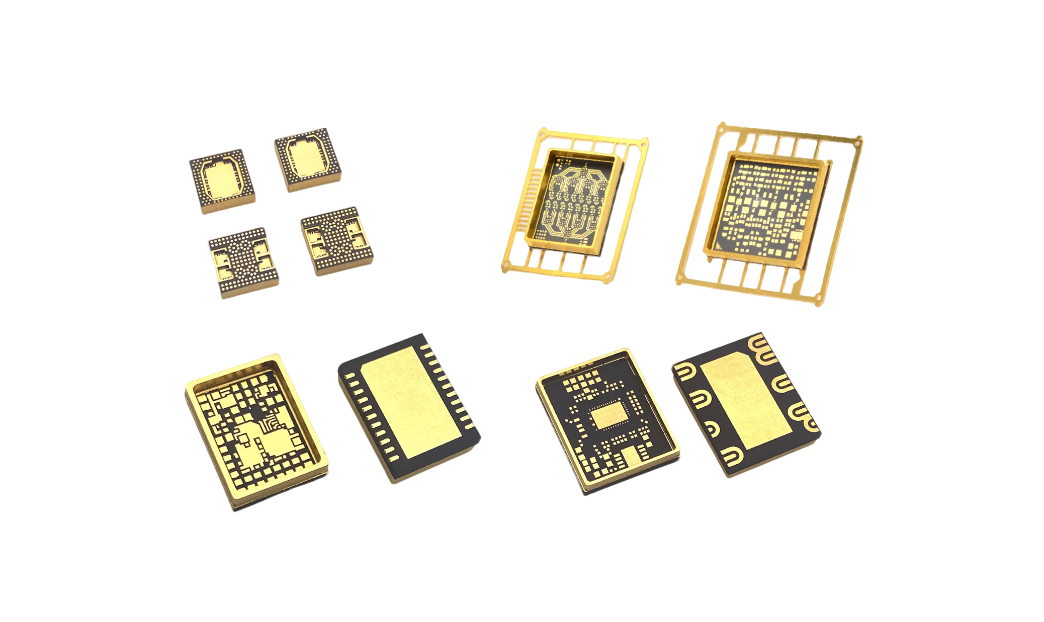
- This type of package belongs to an integrated encapsulation structure, typically used for implementing System-in-Package (SIP) modules.
- The module integrates the substrate and encapsulation into a single unit, internally housing multiple components such as RF circuits, DSPs, ADCs, DACs, SRAM, CPUs, FPGAs, and passive components (resistors, capacitors, etc.).
- This architecture enables higher packaging density and superior system performance. Compared to conventional metal packages combined with MCM-C substrates, it offers advantages including smaller size, higher packaging density, lighter weight, and excellent electrical performance.
- Customizable according to customer requirements.
- Supports 3D interconnect routing, high-density circuit integration, and high packaging efficiency.
- Customized structural design with flexible solder joint layout options.
- Utilizes multi-layer co-firing technology, resulting in compact physical dimensions.
- Fewer solder joints and shorter interconnect paths contribute to outstanding electrical performance.
- High thermal conductivity with customizable heat sink structures to meet diverse thermal management needs.
- High reliability and excellent hermeticity.
- Significant cost advantage compared to LTCC (Low-Temperature Co-fired Ceramic) technology.
Applications
- Primarily used in high-density integrated circuit systems such as RF circuits, digital signal processing, and high-performance analog circuit integration, representing one of the key development trends in current system integration.