Features & Applications
HTCC Materials
HTCC Board Rules
Parameters
Features & Applications
Features
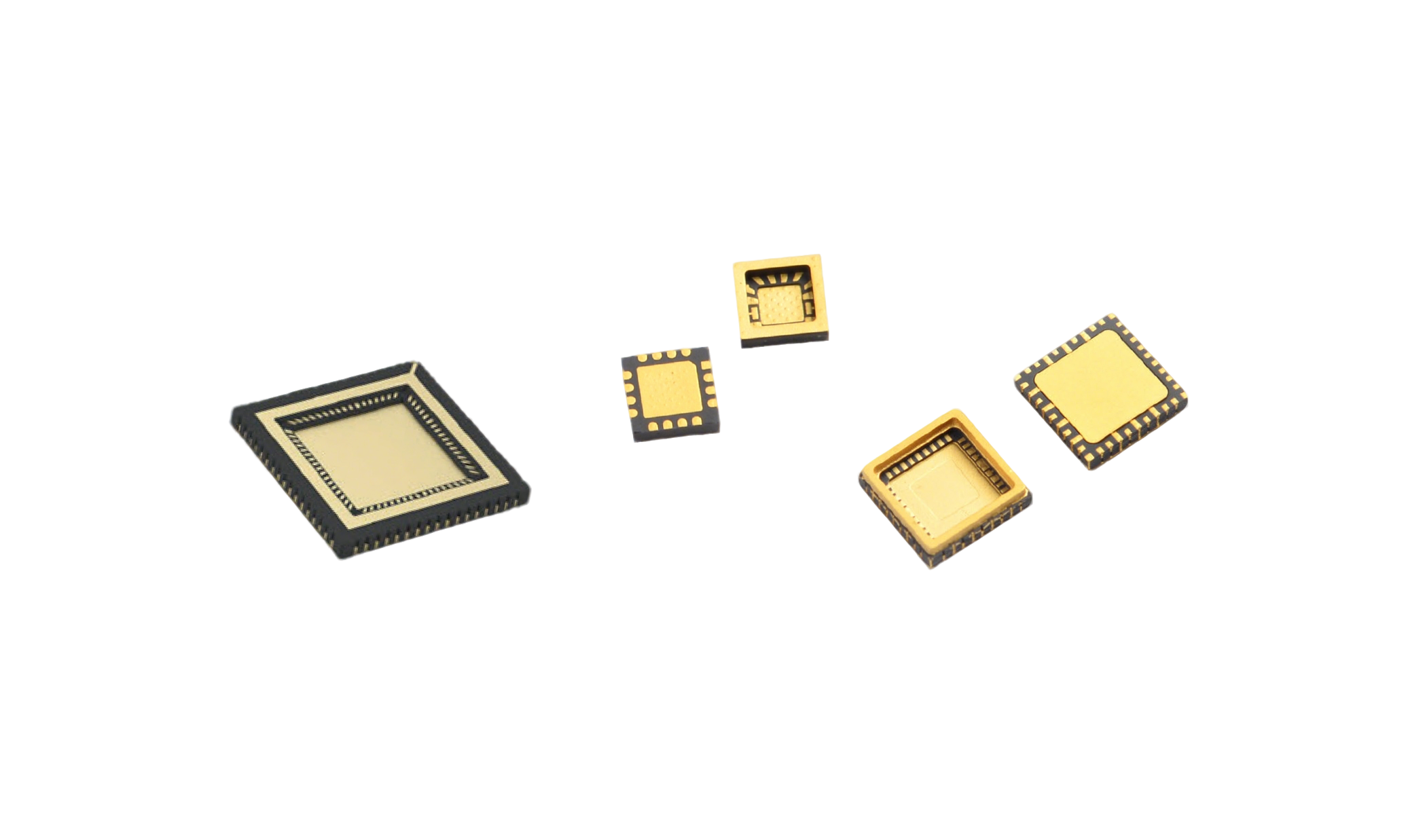
- Features symmetric leadless pads on all four sides, capable of transmitting control signals or RF signals from DC to 40GHz.
- Die attach grounding methods include metallized grounding or metal heat sink grounding to meet diverse thermal management requirements of different chips.
- Package sealing options encompass parallel seam welding, alloy soldering, adhesive bonding, and various other lid attachment methods.
- Compact size, lightweight, excellent high-frequency performance, ideal for packaging low-power chips.
Applications
- Applications include SIP (System-in-Package), optical communication modules, MEMS chips, FPGA packaging, CMOS image sensor packaging, automotive electronics, aerospace and other high-reliability chip packaging solutions, as well as millimeter-wave HTCC (High-Temperature Co-fired Ceramic) substrates.