Features & Applications
HTCC Materials
HTCC Board Rules
Parameters
Features & Applications
Features
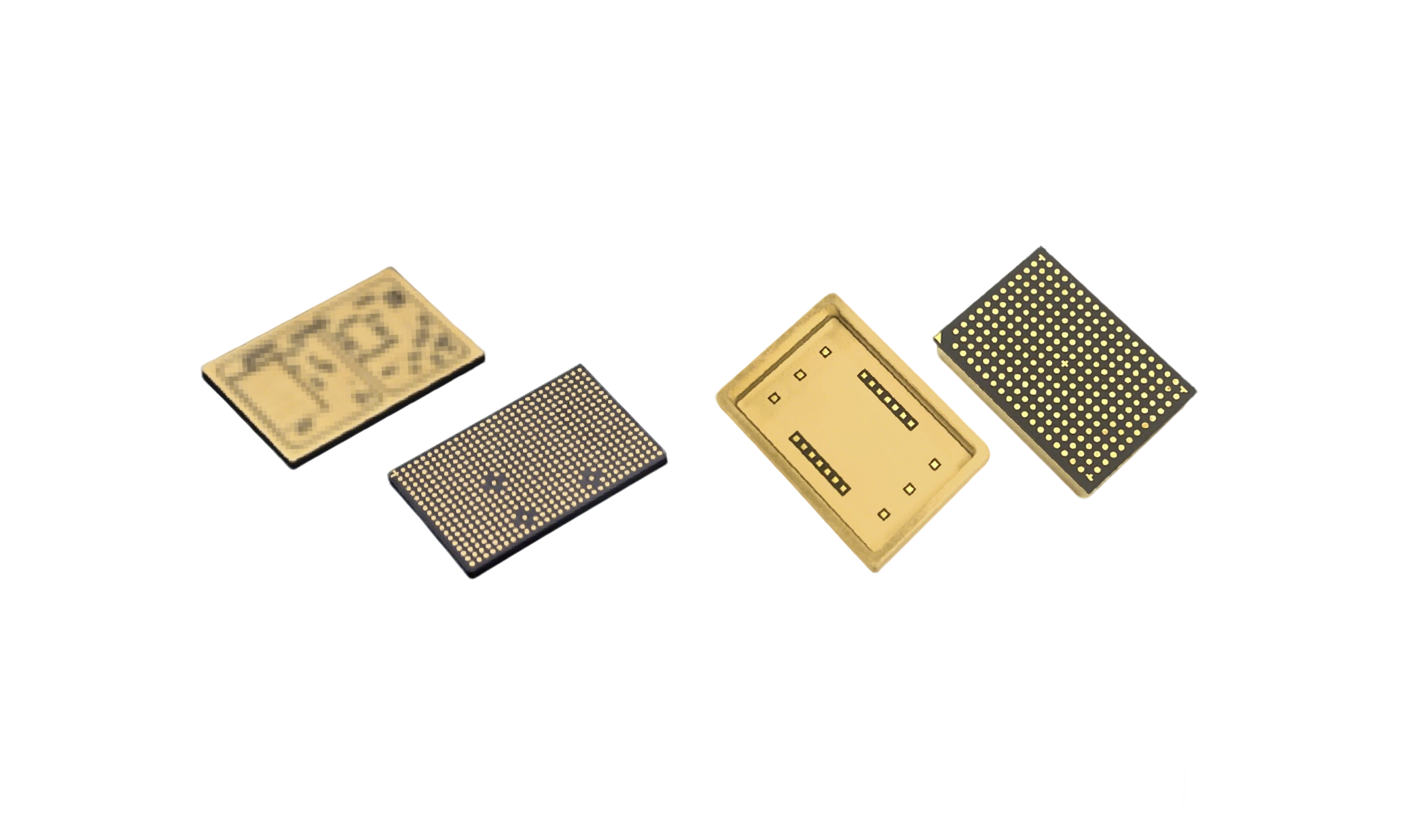
- Spherical solder bumps are fabricated in an array pattern on the package backside to replace traditional leads/pins.
- Terminal pitch is adjustable based on die area, typically 1.27mm, 1mm, or 0.8mm; customizable per customer requirements. A heat sink can be optionally integrated depending on the chip's power dissipation needs.
- Compact size, excellent thermal dissipation, superior moisture resistance, and high reliability.
Array Configurations
- 7×7, 8×8, 10×10……20×20, or customized according to customer specifications.
Applications
- Applications include SIP (System-in-Package), optical communication modules, MEMS chips, FPGA packaging, CMOS image sensor packaging, automotive electronics, aerospace and other high-reliability chip packaging solutions, as well as millimeter-wave HTCC (High-Temperature Co-fired Ceramic) substrates.